TGV Microelectrode Technology

TGV (Through-Glass Via)
Micro through-electrode technology for glass substrates
TGV (Through-Glass Via) is a technology that forms fine through-holes in glass substrates using laser-induced surface modification and etching.By leveraging the intrinsic properties of glass—such as high insulation, low dielectric constant, and low thermal expansion—it is suitable for high-frequency applications, optical communications, and 3D integration.These characteristics position TGV as a next-generation interposer technology capable of replacing TSV (Through-Silicon Via).


High-precision processing ×
Versatile technological support
Processing Methods
LPKF LIDE
Accuracy
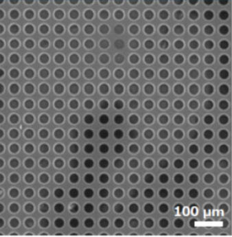
Hole diameter: 20 μm and above / Aspect Ratio: up to 10 / Crack-free processing
Compatible Glass Types
Eagle XG / TEMPAX / Alkali-free and borosilicate glass
Size
From 100 mm (square or round) up to 510 × 515 mm, with ongoing expansion
Prototyping to Mass-Production Capability
Cleanroom-based processes with integrated plating and cleaning
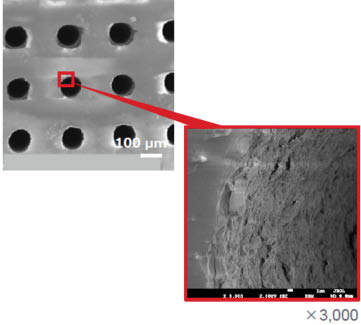
High-Quality Through-Hole Machining
Advantages of the EBINAX LIDE Process
| EBINAX LIDE Processing | Laser Processing | Blast Processing | |
|---|---|---|---|
| Hole Diameter (<100 μm) |
〇 | 〇 | △ |
| Accuracy | 〇 | 〇 | △ |
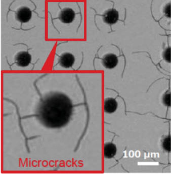
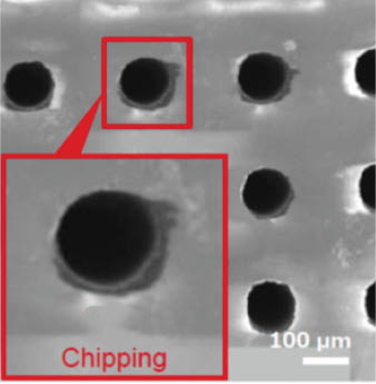
| Crack / Defect Incidence | Very Low | High | Moderate |
| Sidewall Surface Roughness | 〇 | 〇 | △ |
| Glass Surface Image (100 μm) |
 |
 |
 |
| Through-Hole Sidewall Roughness | 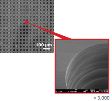 Ra ≦ 0.08μm Ra ≦ 0.08μm |
 |
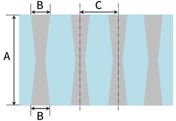
TGV Design Rules
| Glass Substrate Size | 100 mm (Square or Round) Up to 510 × 515 mm, with Ongoing Expansion |
| Glass Thickness (A) | 〜 1000 μm |
| Via Hole Diameter (B)μm | 20 μm 〜 |
| Hole Pitch (C) | > B |
| Aspect Ratio (= B : A) | < 10 *Consultation Required for Aspect Ratios Above 10 |
| Hole Position Accuracy μm | ± 5 |
| Through-Hole Shapes | Straight, Hourglass, Tapered |
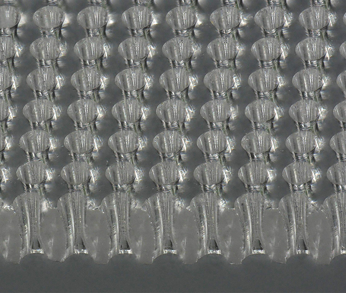
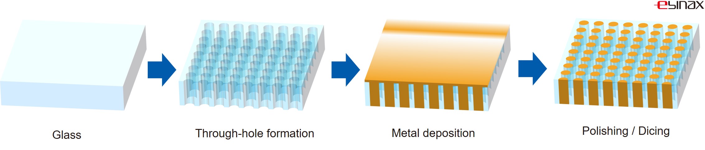
Cross-Section of Through-Glass Vias
Examples of Plating on Glass
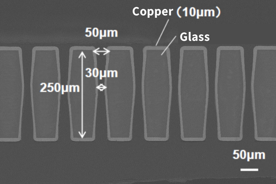
Conformal Plating
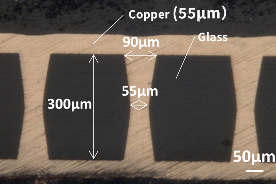
Filled Plating
EBINAX’s through-hole processing delivers exceptionally high quality by minimizing cracks and chipping.
Conventional laser processing and shot blasting tend to generate fine cracks and chipping around the holes, often leading to issues in subsequent plating and electrode formation.
EBINAX minimizes damage around the holes through careful optimization of laser irradiation methods, processing conditions, and etching steps, enabling stable formation of fine through-holes with clean, well-defined profiles.
Our approach maintains dimensional consistency and downstream process compatibility even in high-density TGV designs with micro-vias.
These advantages include:
- Crack-free structures that stabilize downstream processes,
- Chip-free edges that ensure reliable electrode adhesion,
- High-density via layouts that support the advanced performance required for next-generation devices.
Together, these factors are critical enablers for next-generation devices based on TGV technology.
Technical Data / Specifications
| Item | Specification | Notes |
|---|---|---|
| Hole Diameter | Φ20 μm and Above | High Aspect Ratio Available |
| Glass Thickness | 0.1 to 1.0 mm | Thin-Substrate Compatible |
| Processing Method | LIDE / Etching Combination | Optimized According to Application |
| Key Features | Crack-Free / Mass-Production Stability / High Surface Smoothness | Ra ≤ 0.08 μm |
| Supported Sizes | 510×515 300×400 □320 □310 □250 □100 Φ300 Φ200 Φ100, etc. |
Compatible Up to 12-Inch |
| Compatible Substrates | TEMPAX Eagle XG OA-11 Synthetic Quartz PYREX (SG3.3) |
Please contact us for other glass types. |


End-to-End Capability from Material Procurement to Microfabrication and Post-Processing
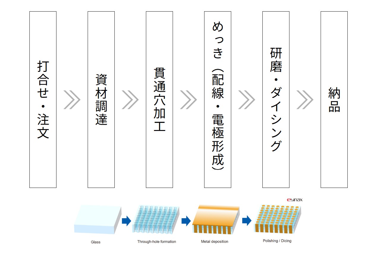
- Consultation and Order Placement

- Material Procurement
- Through-Hole Processing
- Plating (Wiring and Electrode Formation)
- Polishing and Dicing
- Delivery

EBINAX provides comprehensive, end-to-end management for TGV substrate manufacturing.
From initial consultation and specification review through glass procurement, fine through-hole processing, metallization via plating for wiring and electrode formation, finishing processes such as polishing and dicing, and final inspection and delivery, all processes are managed in an integrated manner.
After carefully reviewing customer requirements—including via diameter, pitch, substrate size, glass material, and film thickness—we select the optimal processing methods and materials. Glass materials suited to each application, such as Eagle XG and TEMPAX, are then procured, and crack-free through-holes are formed using laser-induced modification and precision microfabrication equipment.
Following cleaning, seed layer formation and plating processes are applied to the glass substrates to create electrode structures and wiring patterns, ensuring reliable conductivity and strong adhesion. To achieve high-precision finishing of the fabricated TGV structures, final processes such as polishing and dicing are performed, followed by evaluation of electrical characteristics, dimensional accuracy, and visual appearance prior to delivery as finished products.
By managing all of these processes in an integrated manner, EBINAX minimizes process variation, improves yield, shortens lead times, and ensures stable quality—one of our key strengths that enables smooth support from prototyping through mass-production ramp-up.
EBINAX’s R&D and Mass-Production Capabilities
In-House Execution from Technology Development to Mass Production
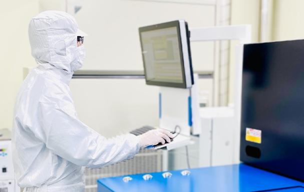
In-House Prototyping, Evaluation, and Analytical Facilities
To accelerate development from prototyping through mass-production validation, EBINAX maintains dedicated in-house prototyping and evaluation facilities equipped with a wide range of analytical tools, including optical microscopes, film thickness gauges, surface roughness measurement instruments, and profilers.
Our in-house infrastructure enables real-time optimization of processing conditions and immediate quality feedback, resulting in shorter development cycles and high process reproducibility.
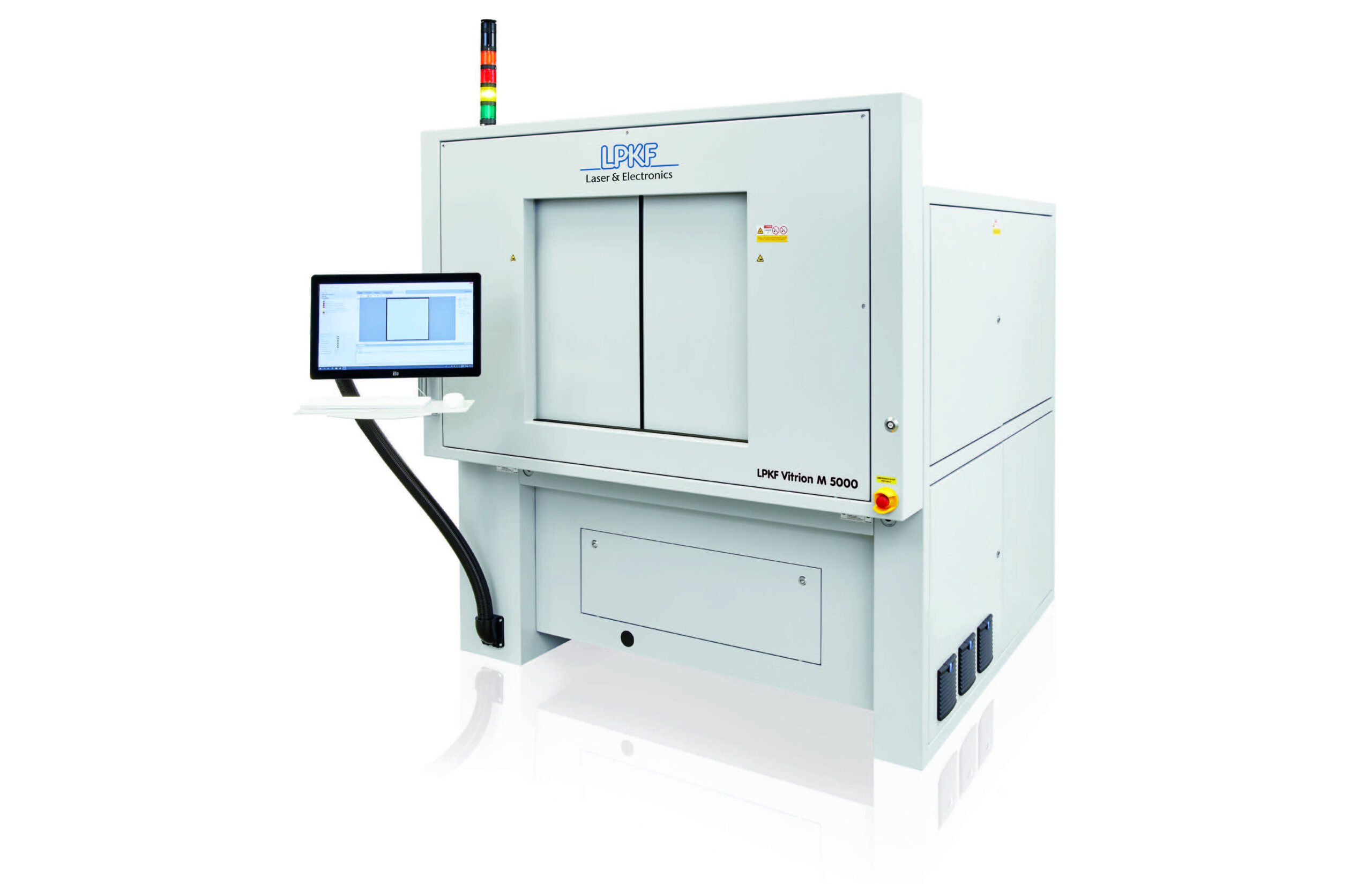
Operation of LPKF LIDE Equipment and Laser Systems
For laser processing, which plays a central role in TGV formation, EBINAX employs LIDE (Laser Induced Deep Etching) systems from LPKF and applies optimized processes according to the application.
Our LIDE systems offer excellent precision in modified-layer formation and etching performance, enabling crack-free, high-aspect-ratio, and highly uniform through-holes.
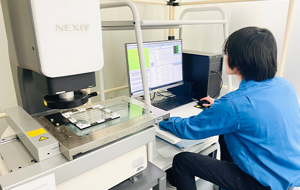
Reliability Testing, Dimensional Analysis, and SEM Observation
After processing, glass substrates are evaluated to verify electrode formation and structural stability through SEM (scanning electron microscopy) cross-sectional observation, dimensional analysis, and surface condition assessment.
We maintain in-house capabilities for reliability testing of wiring conductivity, durability, and adhesion, and provide the verification data required for final product quality assurance.
For Prototyping and Specification Consultation
Inquiries are welcome at any stage of your project.
Please feel free to contact us even if your specifications have not yet been fully defined.