Glass Substrates for High-frequency Circuit Boards
Circuit boards with reduced transmission loss at higher frequencies
What are High-frequency Circuit Boards?
High-frequency circuit boards are a type of PCB which is used in applications involving high-frequency signal transmission between objects
High-frequency Signal
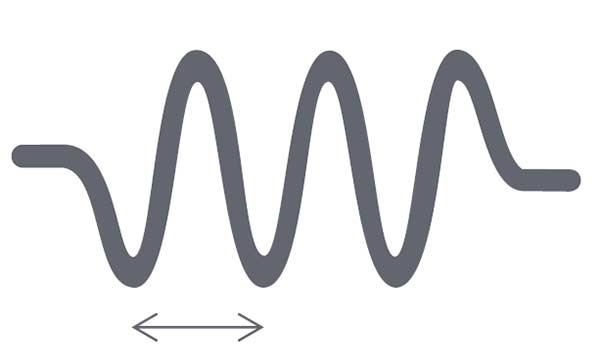
High-frequency:higher than 1GHz
Bandwidth:less than 1m
Applications
5G

3.6~6GHz
28GHz
Mobile
Autonomous cars

79GHz
IoT

Disadvantage
・Easily attenuated by transmission loss
What is transmission loss in HF?
Attenuation per unit-length of high frequency signals
-
Dielectric loss
The loss that occurs when an electromagnetic wave propagates through a dielectric substrate
-
Conductor loss
The losses of circuit resistance and skin effect*
Material and the wiring structure are important for reducing transmission loss
*The “skin effect,” a phenomon in which alternating current avoids travelling through the center of a solid conductor, limiting itself to conduction near the surface
Comparison with Substrate Materials
Comparison with Substrate Materials
Because of its low thermal expansion, glass has superior dimensional stability and superior high frequency transmission characteristics.
| Ref. Silicon | Glass | Ceramics | Organic | ||||
|---|---|---|---|---|---|---|---|
| Alkali-free | Quartz | Al2O3 | AlN | FR-4 | PTFE | ||
| Coefficient of thermal expansion ×10-6/K |
3.9 | 3-4 | 0.5 | 7 | 4-5 | 20 | 7 |
| Permittivity εr |
12 | 5-7 | 4 | <10 | 9 | 4.5 | 2.1 |
| Loss tangent tanδ |
– | 0.002 | <0.0005 | <0.0005 | 0.0005 | 0.005 | 0.0002 |
| Chemical resistance | – | ||||||
| Features | – | high-frequency | Heat dissipation | Low cost | high-frequency | ||
■Good
■Average
■Poor
Reference values
Reference values
Comparison with Dielectric Loss of Substrate Materials
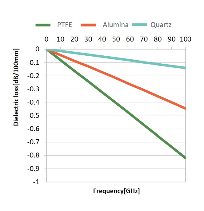
The dielectric loss of quartz
glass is about 1/6 of PTFE *
*on 79GHz Band
■ Simulation results on a microstrip line
■ Permittivity/Loss tangent
● PTFE
(2.6 / 0.0007)
● Alumina
(9.8 / 0.0002)
● Quartz
(3.78 / 0.0001)
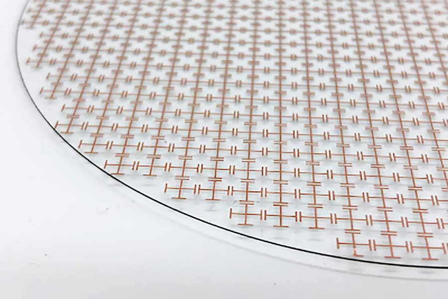
Design Specs
Standard Design
| Glass Size | φ ~8 inch | ||
|---|---|---|---|
| Thickness (A) | 200-600 μm | ||
| Copper Thickness (B)μm | 5 | 10 | 20 |
| Line (C)μm | 10 | 10 | 10 |
| Space (D)μm | 20 | 25 | 50 |
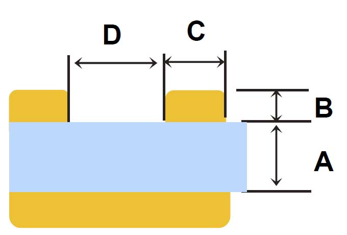
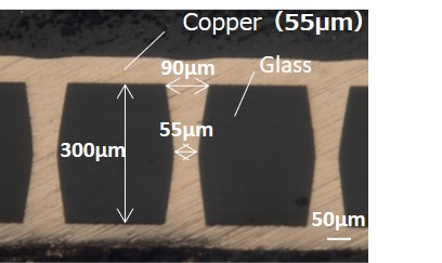
Cross-section
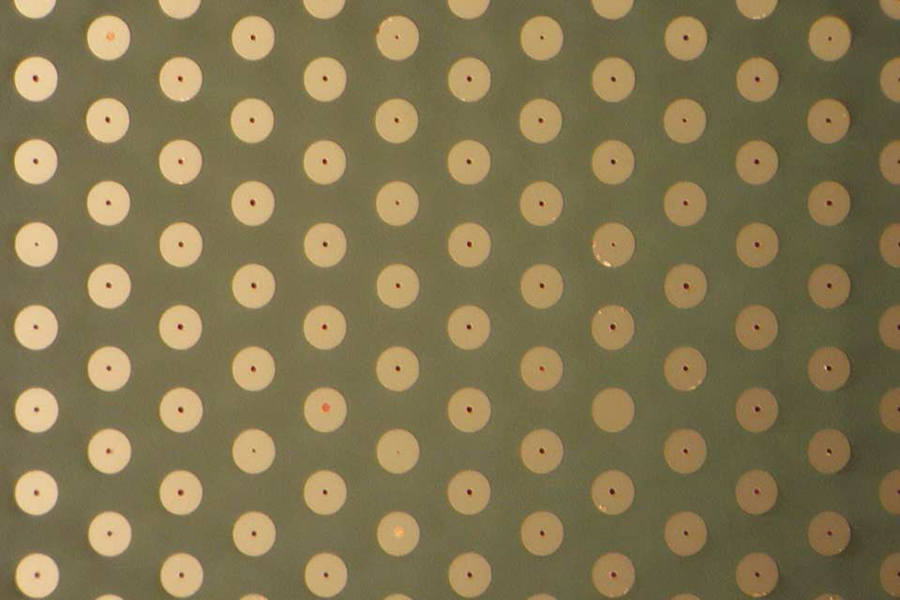
Through-hole Filling
【Actual value】
Via’s Top Diameter (E) 30 μm/Glass Thickness (F) 200 μm
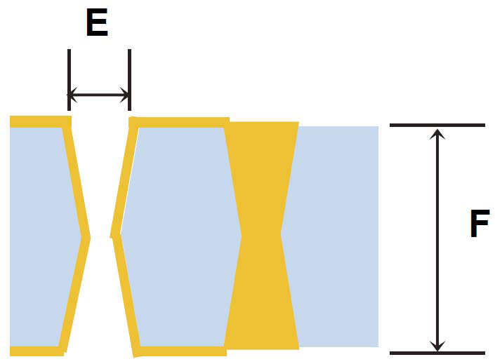
Through-glass via cross-section
Substrate Material
Alkali-free glass / Quartz glass / Borosilicate glass / Soda lime glass / Sapphire glass
These dimensions are for reference only. Please contact us with your exact specifications.
Plating Examples
Wire Plating
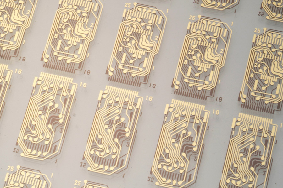
Plating into Through-holes
Cross section
![]()
Through-glass via cross-section
Application Examples
| Purpose | Applications | Fields |
|---|---|---|
| Conduct electricity | interposers(TGV) | Semiconductors, Electronics, Electrical applicances, Telecommunications, Industrial equipment, Medical |
| High frequency substrates, Communication antennas | Semiconductors, Electronics, Electrical applicances, Telecommunications, Industrial equipment, Medical |
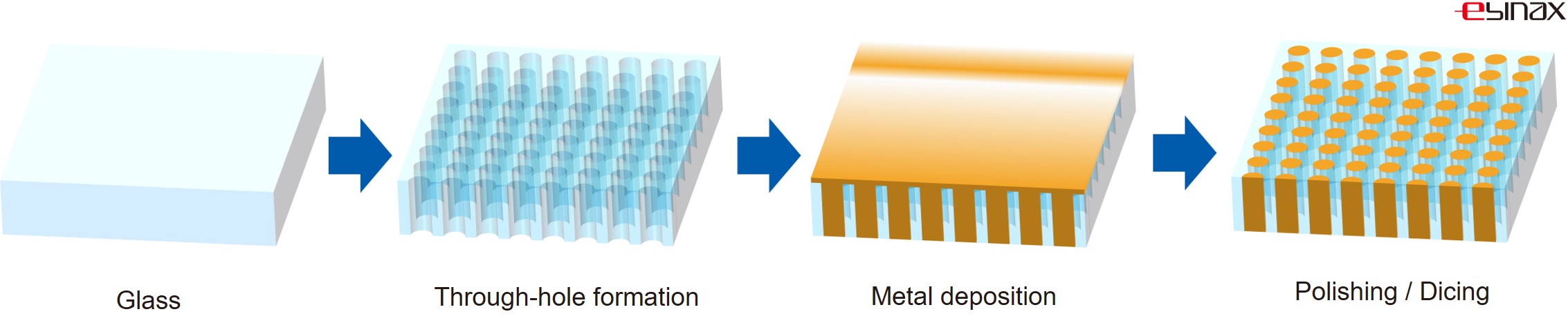
Production Flow Chart
Ebinax has an integrated production system from material procurement to dicing glass substrate.
- Consultation / Order
-

- Material procurement
-
- Glass through-hole processing
-
- Plating (electrode formation)
-
- Polishing / Dicing
-
- Delivery

Please contact us with your needs and specifications.
Ebinax’s process leads to lower management costs and shorter lead times.
<< ”Our Technology”