Company Profile
Greetings
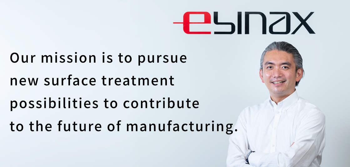
Contributing to the Future of Manufacturing
through Surface Treatment
As a pioneer of next-generation surface treatment,
we lead the industry with cutting-edge R&D
and explore new surface treatment possibilities to contribute
to the future of manufacturing.
We strive to meet the evolving needs of society and our customers
by continuously developing and providing the latest
in cutting-edge surface treatments.
President's Signature
Shinya Ebina
Company Profile
| Trade Name | Ebina Denka Kogyo Co., Ltd. |
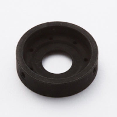
| Business Type | Electroplating and electroless plating on various materials for all industries |
| Representatives | Shinya Ebina, Chief Executive Officer / Kosuke Ebina, Managing Director |
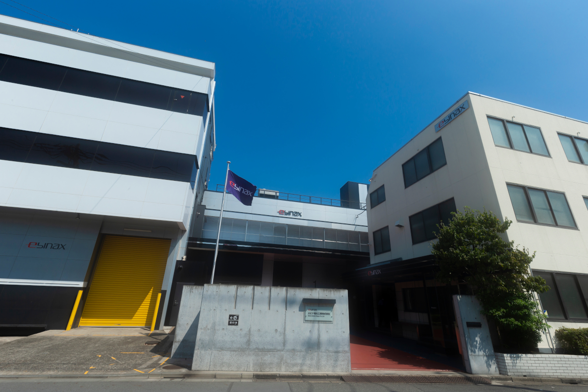
| Head Office Address | 5-22-13 Higashikojiya, Ota-ku, Tokyo 144-0033, Japan |
| Established | November 15th, 1946 |
| Capital | ¥10,000,000 |
| Employees | 100 |
| Our Bank | MUFG Bank, Ltd Kamata-Ekimae Branch |
| ISO | ISO9001 / ISO14001 Authentication office: Head office |
| Awards | 2004: 2nd Annual Courageous Management Awards - Award of Excellence (Tokyo Chamber of Commerce and Industry)2006: Top 300 Innovative Manufacturing SMEs (Ministry of Economy, Trade and Industry - SME Agency)2015: Diversity Management Top 100 (Ministry of Economy, Trade and Industry) |
| Work-Life Balance | In 2014, we registered as a "Tokyo Next-Generation Development Support Company." Through this, we promote work-life balance among our employees to build an environment where they can balance work and child-rearing. |
Company History
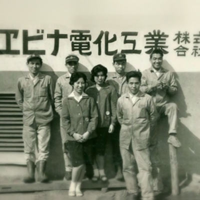
1946

Ebina Plating Factory was established in Ota Ward, Tokyo
1953
Changed the company name to “Ebina Denka Kogyo Co., Ltd.”
1960
Kamata factory was established to expand the production of hard chrome plating and copper-nickel-chrome plating
1964
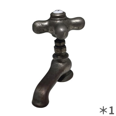
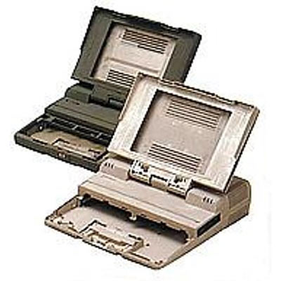
Started production of nickel plating for motorcycle rearview mirrors and water faucets(*1)
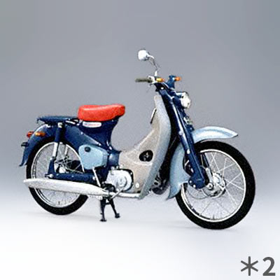
Developed plating process for various plastic materials and started mass production(*2)
1967
Developed plating process for various plastic materials and started mass production
1979
Introduced electroless plating process (kanigen)
1985
Developed plating process for alumina (ceramics) and started mass production
1986
Successfully industrialized EMI shield plating and started mass production
1993
Developed conversion treatment method for magnesium and started mass production
1994
Introduced an electroless plating process able to selectively shield only one side, and started mass production
2002
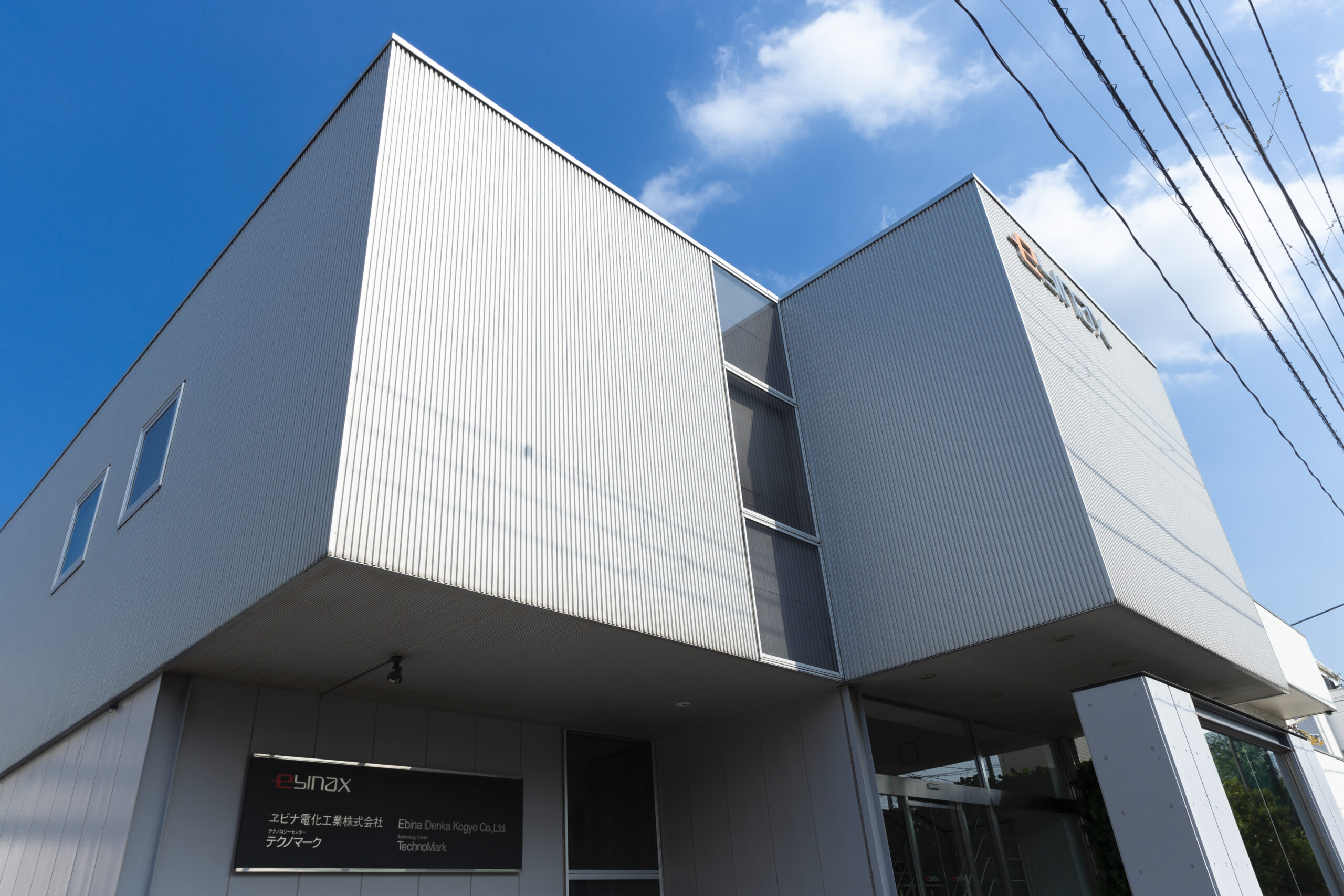
Established “Techno Mark,” the world’s first R&D center specializing in plating technology
2003

Introduced fully automatic plastic plating system to replace metal (Metacarbo Shield Plating Process)
2005
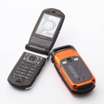
With the spread of mobile phones, began functional plating for antenna parts, in addition to decorative plating for plastic materials
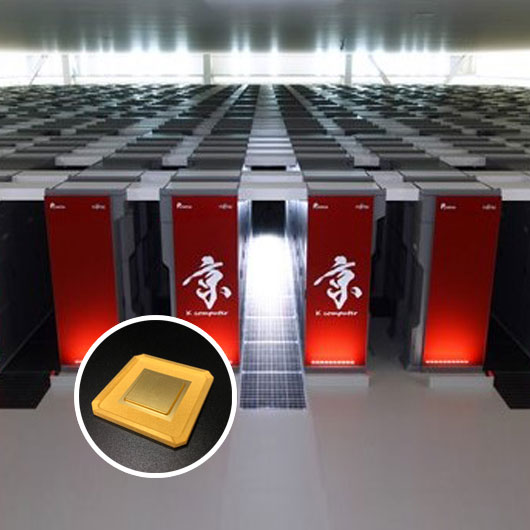
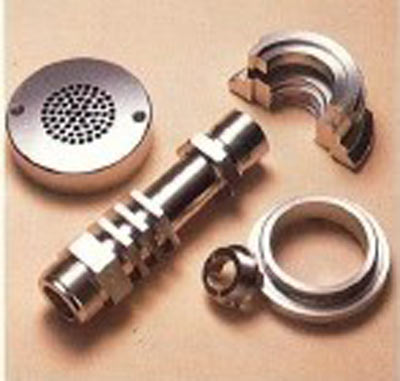
Developed new plating process for AlSiC heat sinks and started mass production(*3)
2009
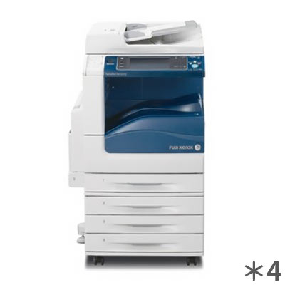
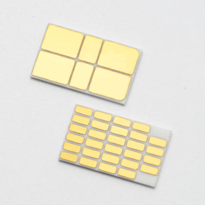
Introduced a fully automatic plating system for heat-sensitive copy machine rollers(*4)
2010
Established “Tech 2,” a new technology center, next to the head factory
2012
Developed "Sugo-Kuro," a plating process using black plating technology
Began operations on antibacterial surface "AGXX"
2014
Began operations on LDS technology "3 Laser Metallization"
2019
Began operations on glass through-hole processing
Installed class 10,000 cleanroom
2021
Formed "METALISM" and opened an innovation lounge in HIcity
*1 Source: Toto Museum
*2 Source: Honda Motor Co., Ltd. and Tokyo Graphic Designers, Inc.
*3 Source:RIKEN Center for Computational Science
*4 Source:FUJIFILM Business Innovation Corp.
Access
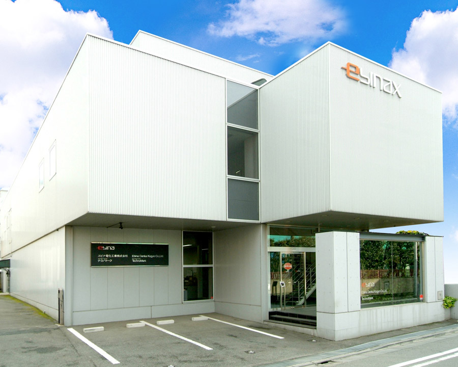
Head Office


Address
5-22-13 Higashikojiya, Ota-ku, Tokyo 144-0033, Japan / TEL +81-3-3742-0107 FAX +81-3-3745-547
Laboratory "Techno Mark"
Address
3-7-22 Nishikojiya, Ota-ku, Tokyo 144-0033, Japan
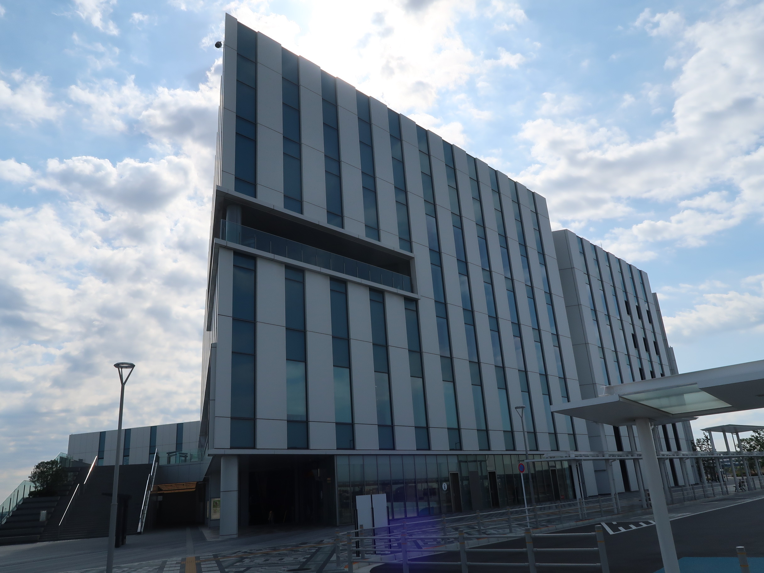
Off-site Lounge "METALISM"(HANEDA INNOVATION CITY)
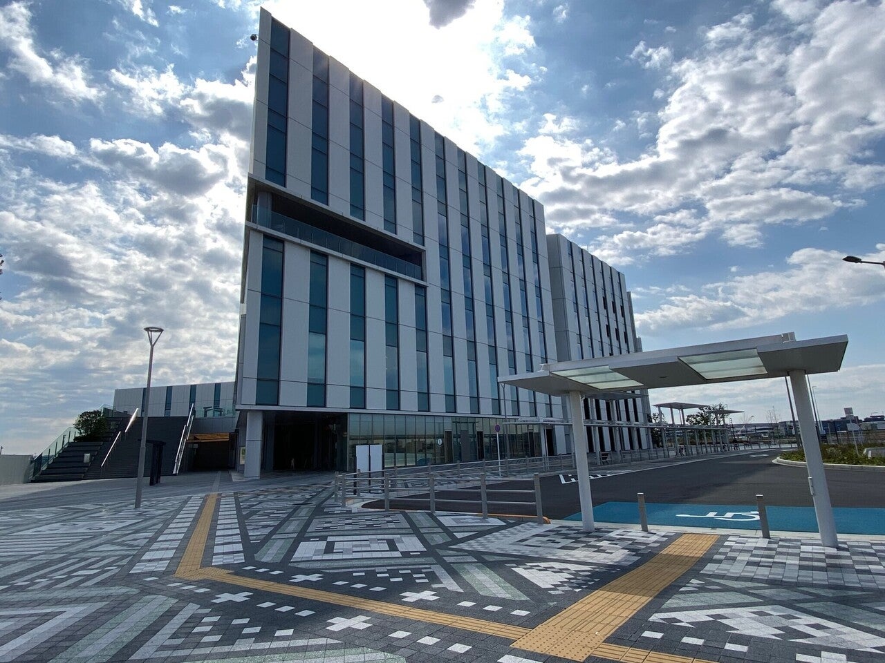
Address
K-208(METALISM), 4-1-1, Haneda Airport, Ota-ku, Tokyo 144-00411, Japan