Ceramics Substrates with Excellent Heat Dissipation
Our plating technology maximizes the performance of semiconductor devices.
Special Features
Provides conductivity and solderability
Various processes based on know-how cultivated over many years
Providing integrated support for all processes starting from the procurement of ceramic substrates
Comparison of Substrate Materials
| Ceramics | Glass | Silicon | Resins | ||||
|---|---|---|---|---|---|---|---|
| Al2O3 | AIN | Alkali-free | Quartz | Silicon | FR-4 | PTFE | |
| Thermal conductivity W/m・k |
30 | 150-250 | 1.0 | 1.3 | 168 | <0.5 | 0.23 |
| Coefficient of thermal expansion ×10-6/K |
7 | 4-5 | 3-4 | 0.5 | 3.9 | 20 | 10 |
| Coefficient of thermal εr |
<10 | 9 | 5-7 | 4 | 12 | 4.5 | 2.1 |
| Loss tangent tanδ |
<0.0005 | 0.0005 | 0.002 | <0.0005 | - | 0.005 | 0.0002 |
| Chemical resistance | |||||||
| Features | Heat dissipation | Excellent high frequency properties | Excellent workability | Low cost | Excellent high frequency properties | ||
■Good
■Average
■Poor
Reference values.
Plating and Patterning Processes
Subtractive Process
Excellent surface mount ability due to flat surface of circuit
- Material
- Seed layer formation
- Electroplating
- Resist formation
- Etching
- Resist removal


- Material
- Seed layer formation
- Electroplating
- Resist formation
- Etching
- Resist removal
Semi-Additive Process
Effective for narrow pitch copper pattern
- Material
- Seed layer formation
- Resist formation
- Electroplating
- Resist removal
- Seed layer removal

- Material
- Seed layer formation
- Resist formation
- Electroplating
- Resist removal
- Seed layer removal
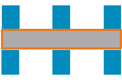
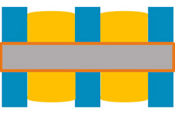
Comparison of Patterning Processes
| Subtractive Process | Semi-Additive Process | |
|---|---|---|
| Shape | 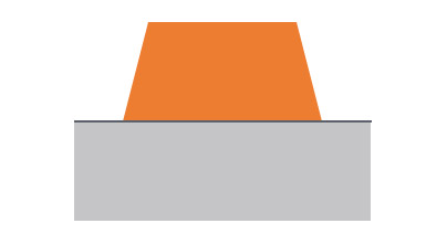 |
 |
| Ease of surface mounting | ||
| Line/Space* | 50/50μm | 10/25μm or more |
| Conductor uniformity in through holes | ||
| Conductivity | ||
| Plating thickness | 50μm or more |
■Good
■Poor
*The value of L/S is based on an example thickness of 10μm.
Design Specs
Ex. Material Specification
Corresponding size: 4 inch
Thickness: 150 – 600 μm
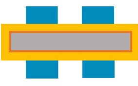
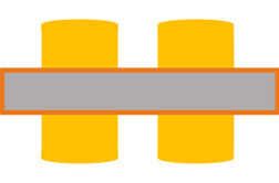
Subtractive Process
| (A) Copper thickness [μm] | 10 | 20 | 50 |
|---|---|---|---|
| (B) Line width [μm] | 50≦ | 50≦ | 50≦ |
| (C) Space [μm] | 50 | 70 | 150 |
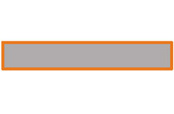
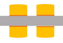
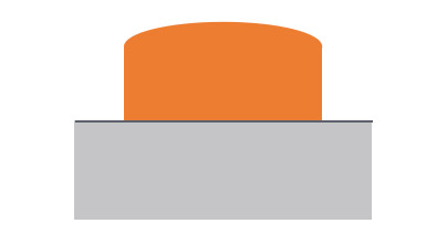
Semi-Additive Process
| (A) Copper thickness [μm] | 10 | 20 | 50 |
|---|---|---|---|
| (B) Line width [μm] | 10 | 10 | 10 |
| (C) Space [μm] | 25 | 50 | - |
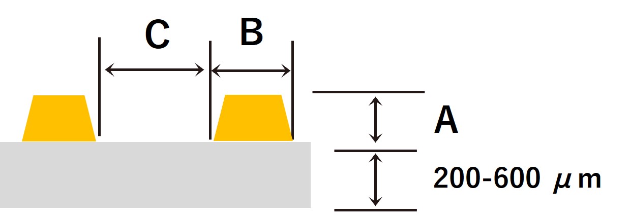
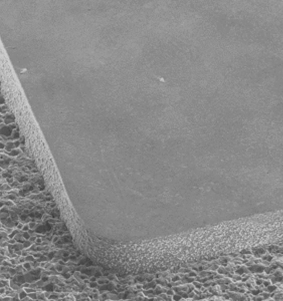
Cross-section(Subtractive)
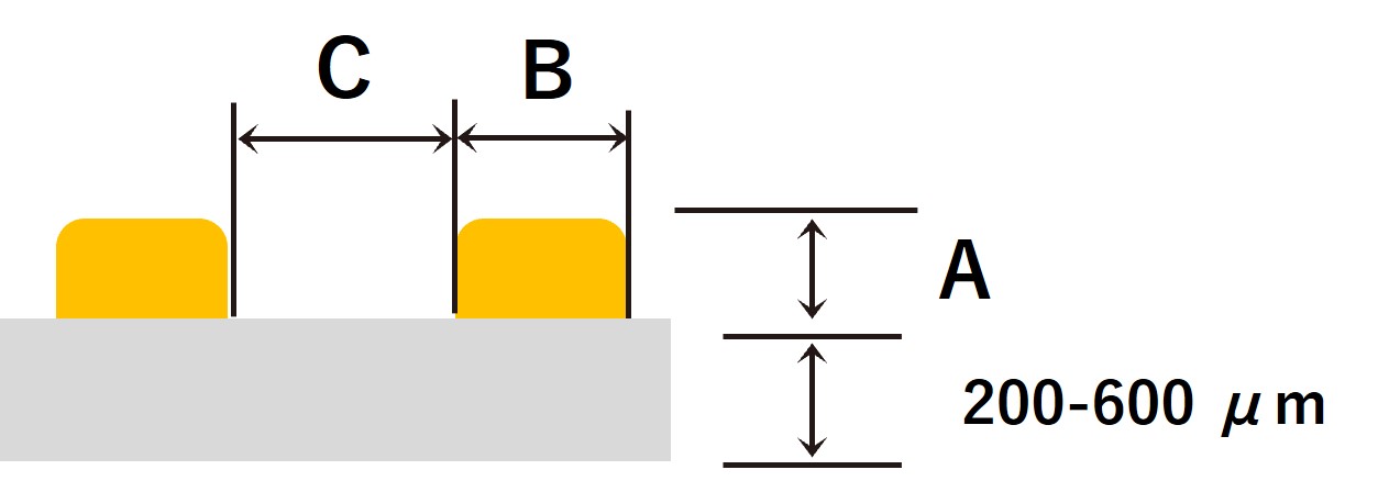
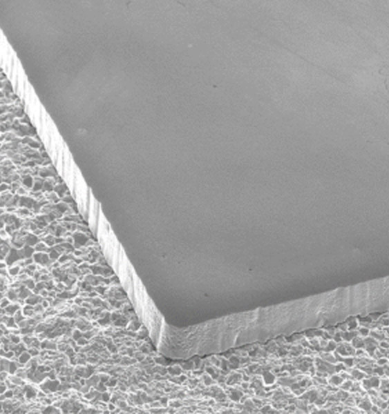
Cross-section(Semi-Additive)
These dimensions are for example only. Please contact us with your exact specifications.
Through-hole Filling
[Actual value]
Via’s top diameter (F) 100µm / Ceramic thickness (G) 300µm
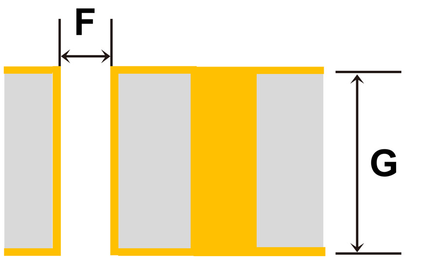
Through-hole via cross-section
These dimensions are for example only. Please contact us with your exact specifications.
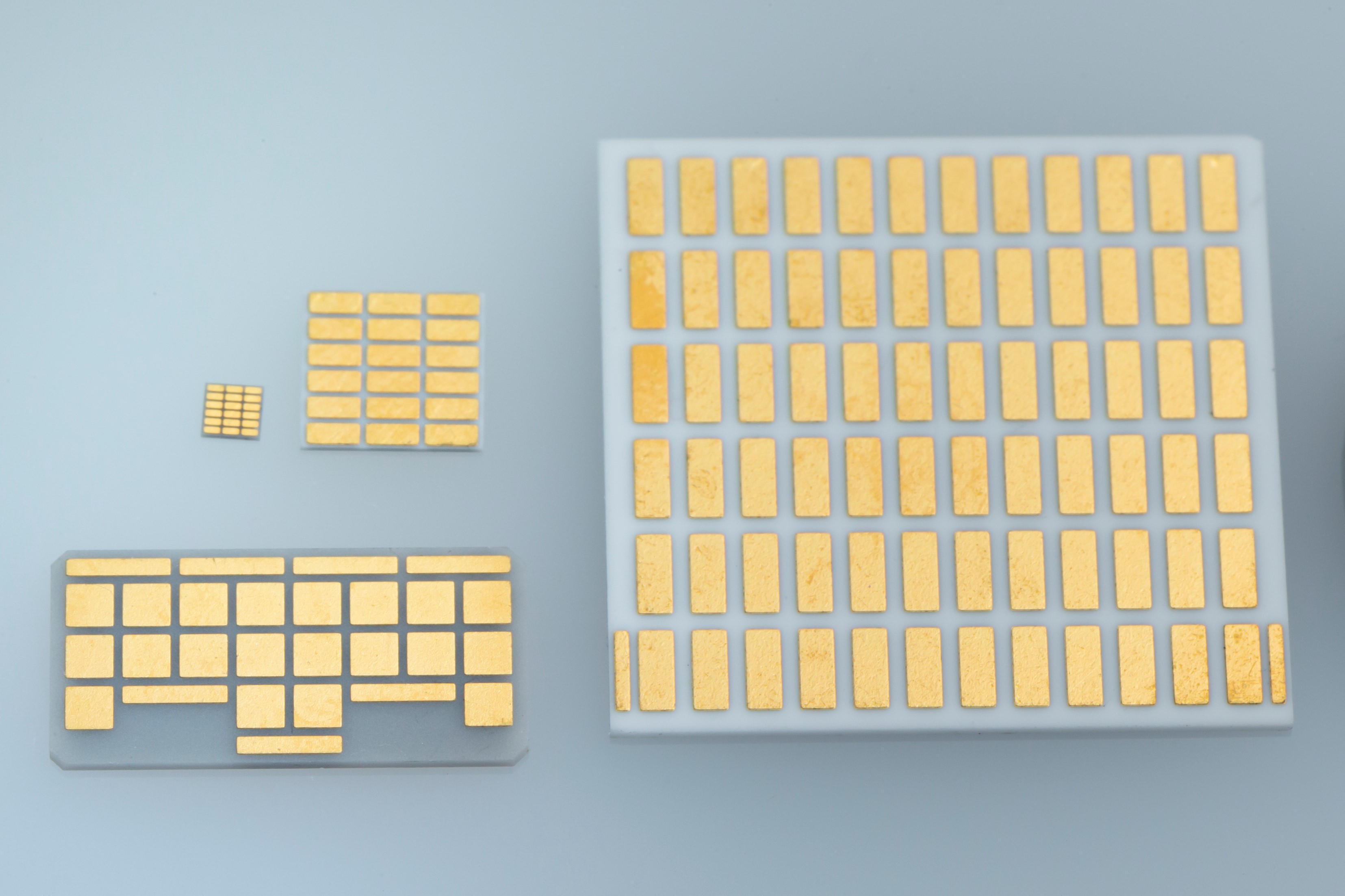
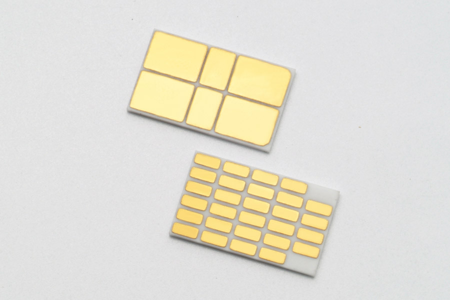
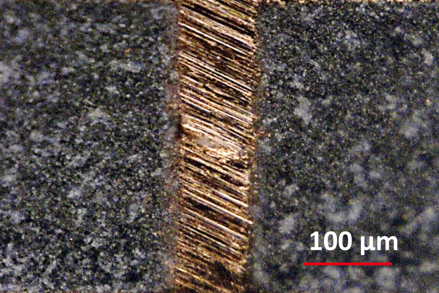
Plating Examples
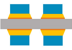
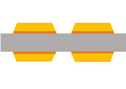
Ceramic Circuit Chip with Selective Plating
Fine pitch wire plating
(Peltier device)
Subtractive process
Semi-Additive process
Through-hole Filling
Substrate Materials and Application Examples
| Type of ceramics | Application |
|---|---|
| Al2O3 | Heat dissipating board, Peltier module |
| ZrO2 | Peltier module |
| ZnO | Semiconductor circuit board, Light emitting diode |
| BaTiO3 | GPS patch antenna, Positive temperature coefficient thermistor |
| PZT | Ink jet printer head |
| AlN | Board for LED, Peltier module, Heat dissipating board |
| SiC | Board laser diode |
| Si3N4 | Invertor, Convertor, Battery, Secondary battery |
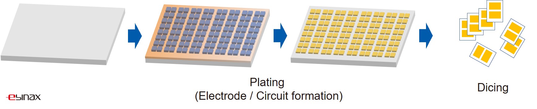
Production Flow Chart
Ebinax has an integrated production system from material procurement to dicing substrate.
- Consultation / Order
-

- Material procurement
-
- Plating (Electrode formation)
-
- Polishing / Dicing
-
- Delivery

Please contact us with your needs and specifications.
Our process leads to lower management costs and shorter lead times.
<< "Plating Technologies"